- Deprecated
- Background
- System outline
- Flowchart
- Top design
- Power rail design
- MCU design
- MISC design
- Design Redundant/Backup strategy
Deprecated
After several meetings with professor, we found that this Radar back-end design is not clear and we need a new design, so I will move on to the SAR Radar Back-end MK2 design. MK1 is deprecated.
Background
Our another goal is mounting millimeter-radar on the drone to conduct SAR imaging. Also, radar is better than either Lidar or stereo camera in bad air condition. It also potentially available to “see through” the obstacle (depends on the material, thickness, surface and much more, but it is possible).
We have a radar module called K-MC1 from RFBeam Microwave GmbH, and since it is just a transmitter with antenna, we need to build back end and signal processing stage making it usable. In this blog, I am going to record my SAR Radar Back-end PCB MK1 design.
System outline
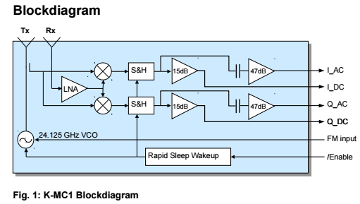
K-MC1 module
K-MC1 is radar transceiver working on 24GHz with 180MHz tuning bandwidth.
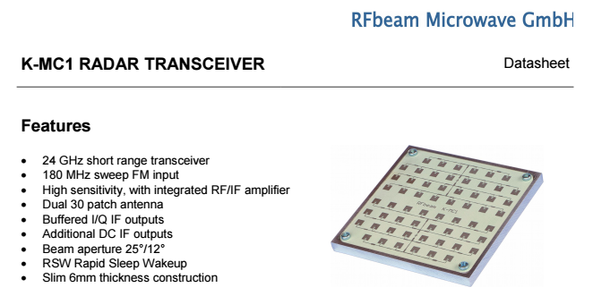
We plan to do the FMCW on this radar, and record the data for signal processing, including SAR imaging.
Support K-MC1 module
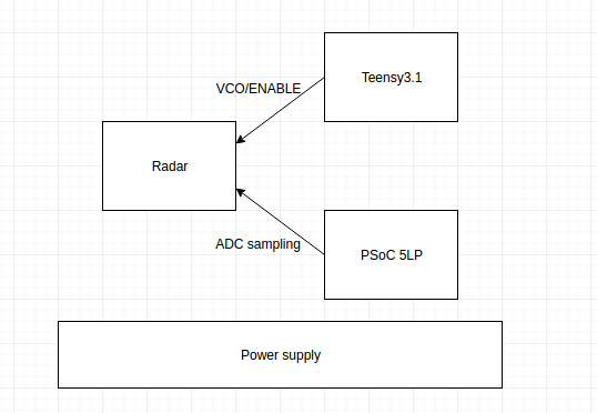
In order to use K-MC1 radar module, we need to provide VCO input, Radar enable signal, and using ADC to read VCO and I_AC output from the module. Dont forget power supply.
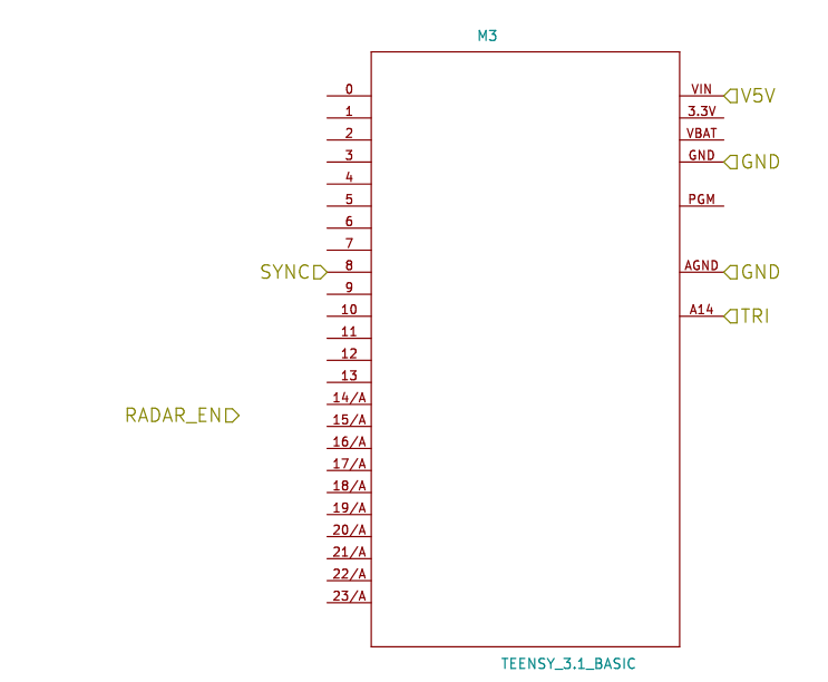
The whole radar system design is collaborative work, and another student is using Teensy 3.1 to provide triangular wave as VCO input, so this back-end PCB top design is like this:
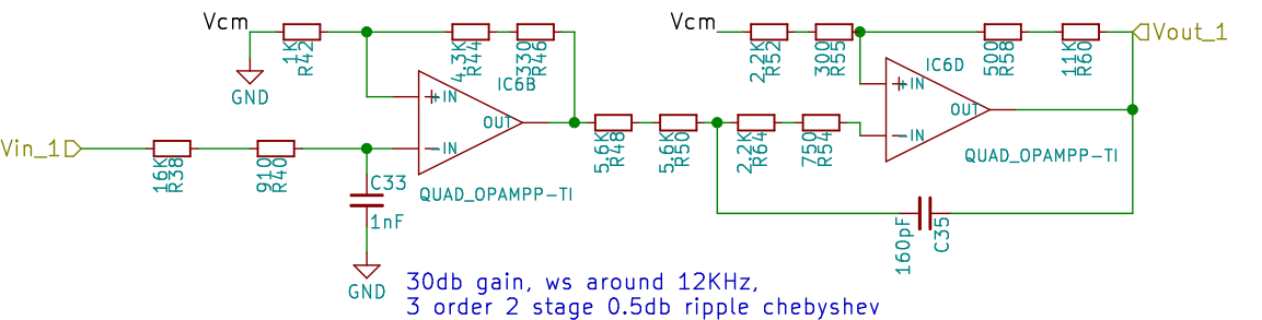
Flowchart
Top design
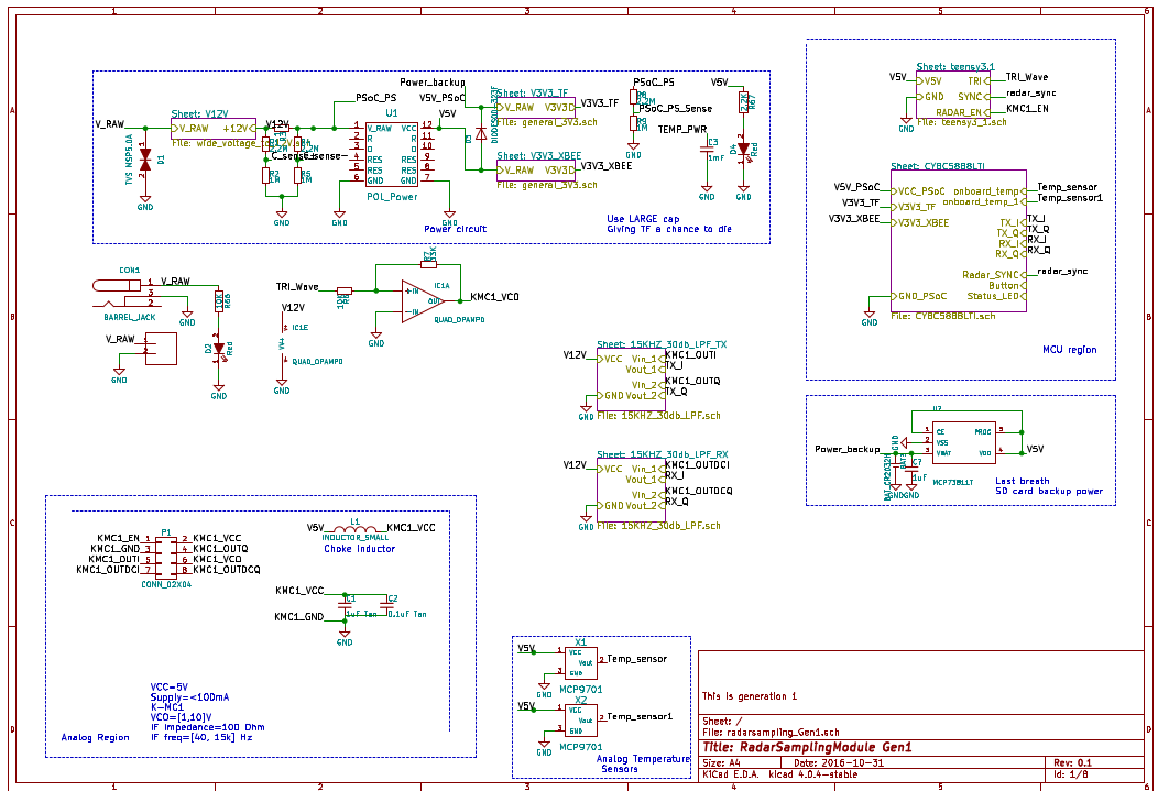
This design has the following features:
- Wide range power input (12~40V)
- SD card data corruption safe battery
- Dual-channel up to 1MSPS(per channel) ADC
- High speed SD card access
- Data transmission over USB2.0 for real-time data processing(PC)
- Parallel output for real-time data processing(2* 10bit+1clock)(DSP/FPGA/etc)
- Selectable signal filter methods
- Selectable VCO source
- ESD protection
- Small footprint
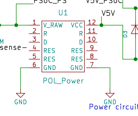
Power rail design
This radar back-end is quite a mix power system with three different voltage rails: 3.3V, 5V and 12V. One thing I need to remind myself is that all of the following power supplies are not enhanced/specialized for RF application, so I need to remember adding enough decoupling and chokes on the RF side. Luckily, we do not need to feed RF frequency signal to the Radar module, so the generalized power supply maybe enough.
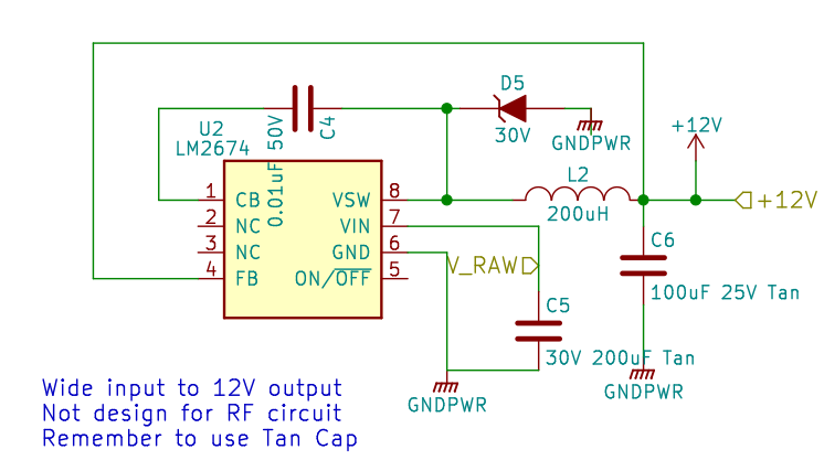
12V rail
Radar requires VCO input with VPP=10V, so 12V rail is provided to power on the opamps to amplifier the TRI wave from Teensy, since Teensy is working under 3.3V voltage.
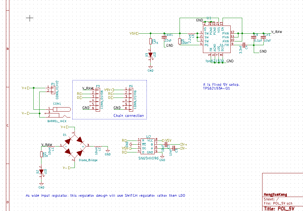
5V rail
5V rail will be provided by my POL 5V module (Power over line), so the schematic looks scared, the actual foot print will be a tiny 12 pins module.
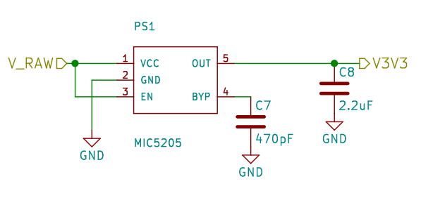
3.3V rail
3.3V rail is major power source for micro SD card, XBee. So in our design, I have two individual 3.3V LDO regulators for each device.
MCU design
Due to the collaboration work, this radar back end design has two MCUs:
Teensy3.1: generating triangular wave VCO signal and radar enabling signal
PSoC 5LP: sampling, interfacing, overall control
Teensy3.1
Since Teensy 3.1 does the basic but essential functionality, I gave it the minimum connection:
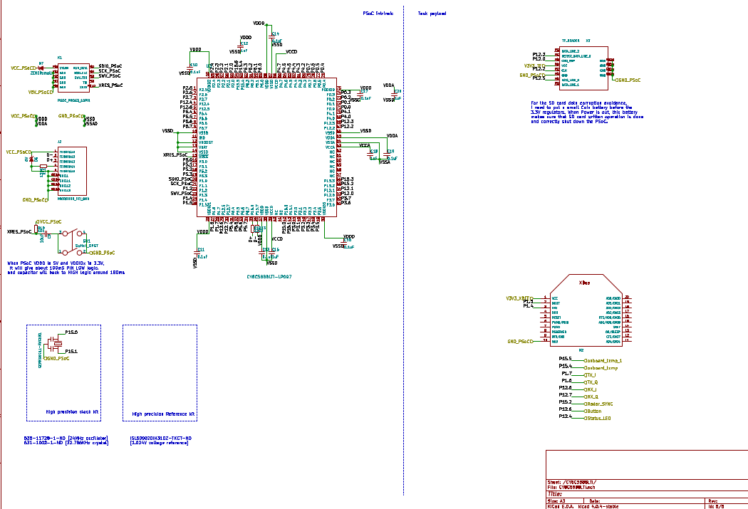
PSoC 5LP
PSoC 5LP design is much more complex, because it will take more responsibilities. (Will explain with more details later)
Last update: Nov.22 2016